ch
ch English

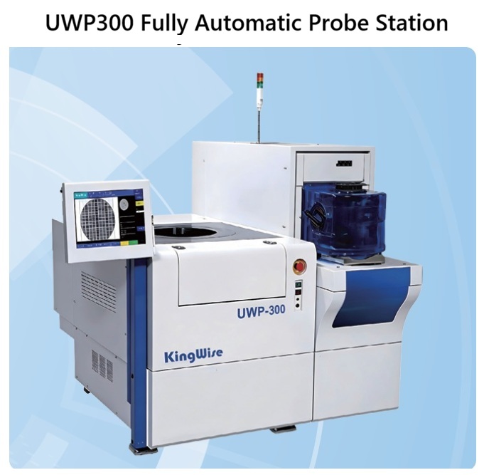
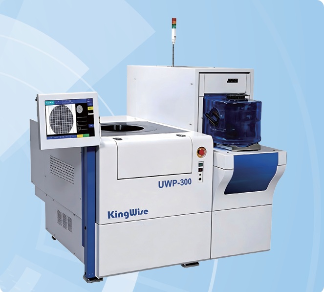
UWP300 Fully Automatic Probe Station
| Equipment Type | UWP300 | |
| Wafer Specifications | Wafer Diameter | 200 mm / 300 mm |
| Thickness (T) | 200μm~2200 μm | |
| Weight | ≤500g | |
| Die Size | 300 μm-100000 μm | |
| XY Axis Specifications | Travel | X:±170mm;Y:-180,+600 mm |
| Accuracy | ≤±1μm | |
| Resolution | 0.1μm | |
| Maximum Speed | 240 mm/s | |
| Z Axis Specifications | Accuracy | ≤±1μm |
| Resolution | 0.1μm | |
| Maximum Speed | 80mm/s | |
| Theta Specifications | Range | ±10° |
| Accuracy | 0.00001° | |
| Cassette /Wafer Size | φ200mmD300mm | |
| Dimensions (L×W×H) in mm | 1600*1660*1450 | |
| Weight (kg) | 2000 | |
| Power Requirement | 50/60 HzAC220V | |
| CDA Pressure | 0.4-0.8 Mpa | |
| Vacuum Pressure | 53-100 Kpa | |
| Overview | Key Features |
| The UWP300 Fully Automatic Probe Station delivers a fully automated wafer-level probing solution, designed as a dual-size compatible test system for both 200 mm and 300 mm standard wafers, supporting Wafer Acceptance Test (WAT) and Chip Probing (CP) applications. The upgraded UWP301 model introduces significant technological enhancements across key performance domains: Automatic Wafer Loading/Unloading and Transport Micron-Level Fully Closed-Loop Motion Control Automatic Wafer-to-Probe Alignment Vision-Based Automatic Calibration High-Speed Feedback Communication Advanced Data Processing Capability These improvements enable the system to deliver a cost-effective, efficient, and stable testing solution tailored to diverse customer requirements across high-volume semiconductor manufacturing environments. | Automatic Wafer Loading/Unloading and Transport Micron-Level Fully Closed-Loop Motion Control High-Strength, Low-Center-of-Gravity Mechanical Design High Precision and Throughput for Enhanced Test Efficiency 7×24 In-Situ Probe CapabilityIntuitive Human-Machine Interface (HMI) |
手机 :(+86)17384554168
邮箱 : rick.lin@osi-tek.com
电话 : 0512-8885-6216
传真 :
地址 : No. 3, Shugang Road, Dongqiao Economic and Technological Development Zone, Ningde City, Fujian Province

Copyright © 2026 All Rights Reserved. 闽ICP备2026020430号-1 XML地图